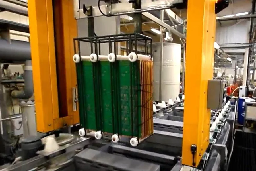
As electronic devices become faster and more complex, maintaining signal integrity has become a critical design priority. Impedance Control PCB technology plays a central role in ensuring that high-frequency signals travel through circuits without distortion, reflection, or loss. By carefully controlling the impedance of traces, these PCBs deliver consistent performance in applications such as telecommunications, automotive electronics, medical devices, aerospace systems, and advanced computing.
Understanding the Concept of Impedance Control PCB
An Impedance Control PCB is designed to maintain a specific impedance level on signal traces throughout the board. Impedance is the opposition that a circuit presents to the flow of alternating current, influenced by trace geometry, dielectric material properties, and PCB layer stack-up. In high-speed or high-frequency circuits, mismatched impedance can cause reflections, timing errors, and data corruption.
To address this, PCB designers calculate and control the impedance of critical traces to match the requirements of components and connectors. Common controlled impedance types include single-ended and differential pairs. Single-ended impedance is typically used for clock signals and other high-speed lines, while differential impedance is crucial for high-speed data transmission protocols such as USB, HDMI, PCIe, and Ethernet.
Importance of Impedance Control in Modern Electronics
The demand for Impedance Control PCB technology has grown rapidly as devices increasingly rely on high-speed communication. Even slight variations in trace width, spacing, or dielectric thickness can result in significant impedance fluctuations, leading to signal integrity problems. By implementing precise control during the design and manufacturing stages, engineers can ensure that signals travel predictably, maintaining timing and minimizing reflections.
Industries like telecommunications and networking depend on impedance-controlled boards to maintain the quality of high-frequency data transfer. In the automotive sector, advanced driver-assistance systems (ADAS) and in-vehicle networks rely on impedance-controlled designs for real-time communication. Medical equipment uses these PCBs to ensure accurate signal transmission in diagnostic and monitoring devices where reliability is paramount.
Key Factors Affecting Impedance Control PCB Design
Designing a reliable Impedance Control PCB involves considering multiple parameters simultaneously. Trace width and spacing are crucial because they directly influence the impedance value. The dielectric constant (Dk) of the PCB material determines how electromagnetic signals propagate through the board. Thicker dielectric layers generally result in higher impedance, while thinner layers lower it.
The layer stack-up configuration also plays a significant role. Controlled impedance is typically implemented on inner or outer signal layers with carefully positioned reference planes to maintain consistency. Differential pairs must be routed with uniform spacing and length matching to preserve signal timing.
Designers use simulation tools and field solvers to calculate impedance accurately during the PCB layout stage. Manufacturers then follow these specifications with tight tolerances to ensure that the final product matches the intended impedance values.
Manufacturing Techniques for Impedance Control PCB
Producing a high-quality Impedance Control PCB requires advanced manufacturing capabilities. Fabricators must maintain strict control over trace geometry, dielectric thickness, and material uniformity throughout the production process. Specialized impedance testers are used to verify that the finished PCB meets the required specifications.
The process typically involves selecting materials with stable dielectric properties, such as FR-4, Rogers, or other high-performance laminates. Precise etching techniques are used to maintain accurate trace widths. Manufacturers also ensure minimal variation during lamination to keep dielectric thickness within tolerance. After fabrication, Time Domain Reflectometry (TDR) testing is performed to measure the impedance of critical traces and confirm compliance.
Applications of Impedance Control PCB Across Industries
Impedance Control PCB technology is used wherever high-speed signals must travel without interference. In data centers and networking equipment, these PCBs support protocols that require strict signal integrity, such as 10G/40G Ethernet and fiber channel systems. Consumer electronics like smartphones and tablets rely on impedance-controlled designs to support USB, HDMI, and high-speed memory interfaces.
In aerospace and defense applications, these boards are essential for radar, communication, and navigation systems, where even minor signal losses can affect performance. Automotive systems use impedance-controlled PCBs in sensor modules, control units, and infotainment networks to enable real-time data exchange.
Partnering with a Trusted Supplier
Collaborating with an experienced Impedance Control PCB supplier is essential to achieve reliable performance in high-speed electronic designs. A skilled supplier can provide precise manufacturing, consistent material quality, and rigorous testing to ensure that the final product meets all impedance specifications.
By choosing the right Impedance Control PCB supplier, you can ensure that your designs maintain signal integrity, reduce development risks, and deliver optimal performance across a wide range of demanding applications.

